
Power MOSFETs can look almost identical from the outside while using very different structures inside the silicon. Two important approaches are Shielded Gate Trench (SGT) and Superjunction (SJ) MOSFETs.
Both aim to reduce loss, but they attack different parts of the silicon power-device problem. Understanding why helps explain a basic rule of power electronics:
There is no single MOSFET structure that is best at every voltage, current and switching frequency.
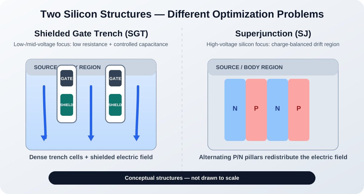
The fundamental silicon trade-off
A power MOSFET has to do two jobs that naturally work against each other:
- conduct current with very little resistance when ON;
- block voltage safely when OFF.
In a conventional vertical MOSFET, higher blocking voltage requires a drift region capable of supporting a stronger electric field. As the required voltage rises, that region generally becomes thicker and more lightly doped.
The penalty is resistance.
That is why high-voltage silicon MOSFET design is fundamentally different from optimizing a device for a 30 V, 40 V or 100 V rail.
What is an SGT MOSFET?
SGT commonly refers to Shielded Gate Trench MOSFET technology.
A trench MOSFET places the gate vertically inside trenches formed in the silicon rather than relying only on a planar surface structure. This creates a compact vertical current path and allows high cell density.
In an SGT structure, a shield electrode is used beneath or adjacent to the active gate region. The shield helps shape the electric field and can reduce the gate-to-drain coupling that would otherwise increase switching loss.
The design objective is typically a strong balance of:
- low
RDS(on); - high current density;
- controlled gate charge and capacitances;
- good switching behaviour;
- compact silicon area.
These characteristics make SGT particularly attractive in low- and medium-voltage power applications.
Why SGT is effective at lower voltages
At lower voltage, the drift region contributes a smaller fraction of total device resistance than it does in a high-voltage MOSFET. Engineers can therefore gain substantial performance by optimizing:
- trench geometry;
- cell pitch;
- channel resistance;
- source and contact resistance;
- gate-to-drain capacitance;
- package resistance.
This is particularly useful in high-current applications because conduction loss rises with the square of current:
Pcond ≈ Irms² × RDS(on)
A few milliohms can therefore make a meaningful difference in battery systems, motor drives, synchronous rectifiers and other low-voltage high-current circuits.
Typical SGT application areas include:
- battery protection and battery-powered systems;
- motor drives;
- power tools;
- synchronous rectification;
- low- and medium-voltage DC-DC conversion;
- consumer appliances;
- automotive low-voltage power distribution.
What is a Superjunction MOSFET?
As voltage increases into the hundreds of volts, the drift region becomes a much larger part of the MOSFET's resistance.
Superjunction technology changes this region fundamentally.
Instead of relying on a conventional lightly doped drift layer, an SJ MOSFET uses alternating P-type and N-type regions or pillars arranged so their charges are approximately balanced.
When the device is OFF, this structure allows the electric field to spread through the drift region more effectively. When the device is ON, the N-type regions can be more heavily doped than in a conventional high-voltage MOSFET.
The practical result is a major improvement in the traditional relationship between:
breakdown voltage and specific on-resistance.
That is why Superjunction MOSFETs became so important for high-voltage silicon switching.
Why Superjunction matters around offline voltages
Consider an AC-DC power supply connected to universal mains.
After rectification and power-factor correction, an internal DC bus may operate around several hundred volts. The switching transistor therefore needs substantial voltage margin above that bus.
Simply scaling a conventional silicon MOSFET upward would make drift-region resistance increasingly unattractive. Superjunction technology allows much better high-voltage silicon performance and is widely used in voltage classes such as 500 V, 600 V and 650 V.
Common application areas include:
- offline AC-DC supplies;
- power-factor-correction stages;
- flyback converters;
- LLC converters;
- adapters and chargers;
- LED power supplies;
- server and telecom power;
- industrial power conversion.
SGT and Superjunction solve different problems
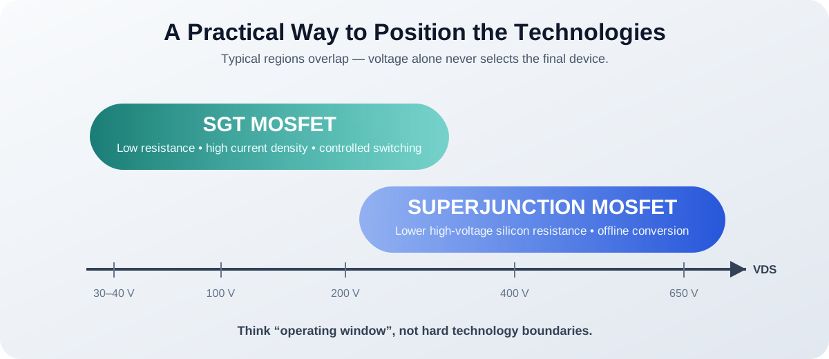
A useful simplified view is:
| Technology | Main optimization | Typical operating region |
|---|---|---|
| SGT MOSFET | Very low resistance, high current density and controlled switching parasitics | Low to medium voltage |
| Superjunction MOSFET | Lower silicon resistance while blocking hundreds of volts | Medium to high voltage silicon switching |
These are not rigid boundaries. Device technology continues to evolve, and commercial products overlap in voltage range.
But the underlying reason remains useful: SGT is generally about extracting better low-/mid-voltage MOSFET performance, while Superjunction addresses the resistance penalty of high-voltage silicon.
RDS(on) is not the whole story
Even within the correct voltage class, the lowest resistance device is not automatically the best switch.
Important dynamic parameters include:
- total gate charge
Qg; - reverse-transfer charge or capacitance;
- output capacitance
Coss; - body-diode behaviour;
- reverse recovery;
- package inductance.
A larger die can reduce RDS(on) but may increase capacitance and gate charge. At high switching frequency, that trade-off can outweigh some of the conduction benefit.
The correct comparison is therefore total system loss, not one headline parameter.
Package technology becomes part of the device
As silicon resistance falls, resistance and inductance outside the active die become more visible.
Loss and switching behaviour can be influenced by:
- leadframe resistance;
- bond wires or clip structures;
- source inductance;
- PCB copper;
- thermal interface;
- package thermal resistance.
Modern packages such as PDFN, LFPAK-type structures, TOLL and TOLT exist partly because high-performance silicon increasingly needs equally strong electrical and thermal interconnects.
A practical selection perspective
For a low-voltage, high-current design, engineers often place heavy emphasis on:
- low hot
RDS(on); - package resistance;
- current capability;
- gate charge;
- thermal performance.
SGT-type MOSFETs often fit this space well.
For a high-voltage silicon converter, priorities shift toward:
- voltage margin;
- high-voltage specific resistance;
- switching energy;
Cossbehaviour;- reverse recovery;
- EMI and transient behaviour.
Superjunction technology is often attractive in this region.
Key takeaway
SGT and Superjunction are not simply two marketing names for better MOSFETs. They represent different engineering responses to different regions of the silicon power-device landscape.
SGT technology is especially useful when low resistance, high current density and good switching behaviour are needed at lower voltages.
Superjunction technology attacks one of silicon's fundamental high-voltage limitations by reducing the resistance penalty associated with blocking hundreds of volts.
Understanding the difference also leads naturally to the next question:
What happens when designers want to push voltage, switching frequency and power density beyond what silicon can deliver economically?
That is where wide-bandgap materials such as SiC and GaN become increasingly important.