
Silicon has powered the electronics industry for decades and continues to dominate an enormous range of power applications.
Modern silicon MOSFETs, Superjunction MOSFETs and IGBTs are mature, cost-effective and highly optimized. So why is the industry increasingly interested in silicon carbide (SiC) and gallium nitride (GaN)?
The answer is not that silicon is obsolete.
The shift is being driven by demanding system goals:
- higher efficiency;
- higher switching frequency;
- smaller size and weight;
- higher operating voltage;
- higher power density;
- reduced cooling burden.
As designers push closer to the practical limits of silicon in particular operating regions, wide-bandgap semiconductors create new system-level options.
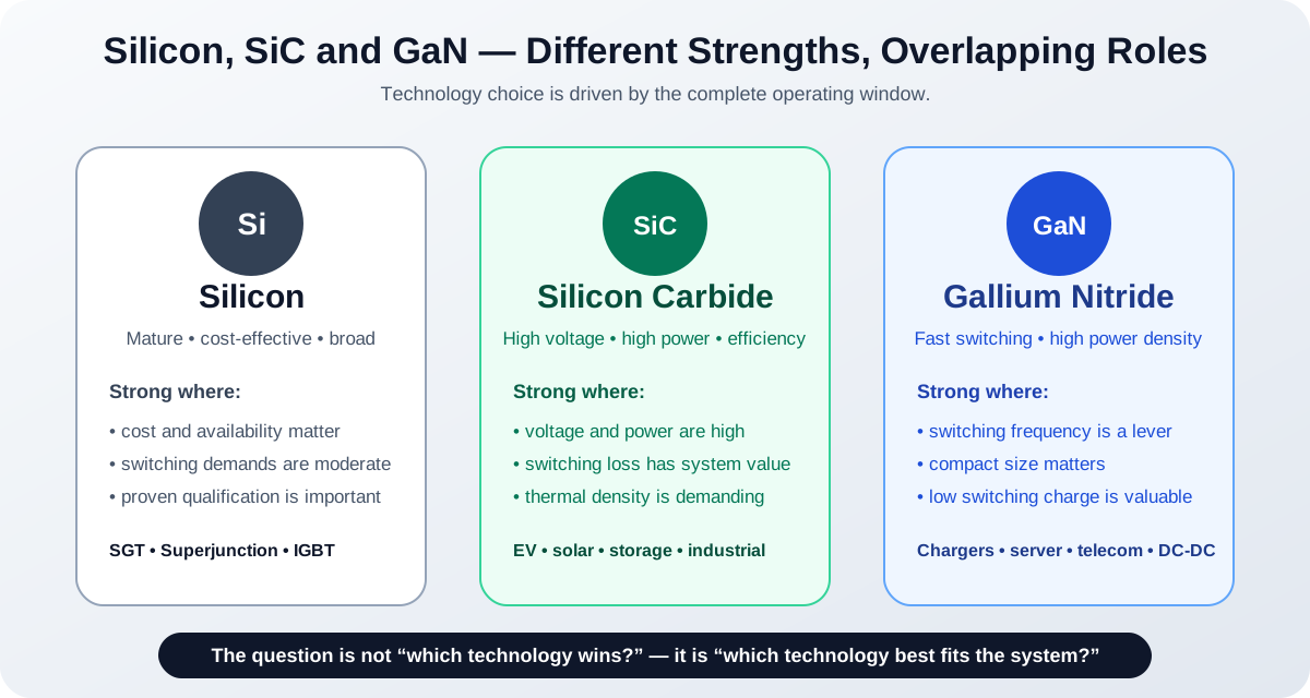
Silicon still matters — a lot
Before looking at SiC and GaN, it is important to recognize how capable silicon has become.
Modern silicon technologies include:
- Shielded Gate Trench MOSFETs;
- Superjunction MOSFETs;
- advanced IGBTs;
- fast and optimized diode technologies;
- low-inductance, thermally efficient packaging.
For many consumer, industrial and automotive designs, silicon still offers an excellent balance of:
- performance;
- cost;
- reliability;
- supply maturity;
- ease of use.
A low-voltage motor drive, a consumer appliance or many industrial converters may have little economic reason to move away from silicon.
The transition to wide-bandgap devices is therefore application dependent, not universal.
Where silicon becomes more difficult
An ideal power switch would have:
- zero resistance when ON;
- infinite resistance when OFF;
- zero switching time;
- zero capacitance;
- unlimited temperature capability.
Real devices must compromise.
As voltage and switching frequency rise, silicon devices face increasingly difficult trade-offs between:
- breakdown voltage;
- on-resistance;
- capacitance and stored charge;
- switching loss;
- die size;
- temperature.
Superjunction technology substantially extended the useful range of high-voltage silicon MOSFETs, and IGBTs remain powerful solutions at high voltage and power. But some applications can gain enough system benefit from a different semiconductor material to justify the change.
What does “wide bandgap” mean?
The bandgap is a basic property of semiconductor material.
Silicon has a bandgap of roughly 1.1 eV, while 4H-SiC and GaN are both around 3.3–3.4 eV.
The wider bandgap contributes to a much higher critical electric field before breakdown. In practical device design, that can enable thinner, more highly doped voltage-blocking regions than silicon for a similar voltage class.
That opens the door to combinations of:
- high blocking voltage;
- lower resistance;
- faster switching;
- higher-temperature capability.
The real benefit, however, is not simply a better transistor. It is the possibility of redesigning the whole converter.
Silicon Carbide: strong when voltage and power rise
SiC has become particularly important in systems involving substantial voltage and power.
Typical application areas include:
- EV traction inverters;
- onboard chargers;
- DC fast charging;
- solar inverters;
- energy-storage systems;
- industrial drives;
- high-voltage power conversion.
Why SiC is attractive
SiC devices can combine high blocking voltage with relatively low switching and conduction losses.
Compared with conventional high-voltage silicon approaches, that can allow:
- higher efficiency;
- lower switching loss;
- higher switching frequency;
- reduced cooling requirements;
- smaller passive components in some topologies;
- higher system power density.
SiC is especially compelling in voltage classes around 650 V, 1200 V and above, although the exact technology choice always depends on topology, power level and economics.
Example: EV traction inverter
An EV traction inverter converts battery DC power into controlled AC power for the motor.
Every watt lost in the switching devices becomes two problems:
- energy taken from the battery without producing motion;
- heat that must be removed from the inverter.
Reducing semiconductor loss can therefore contribute to:
- improved drivetrain efficiency;
- reduced thermal-system demand;
- smaller or lighter cooling hardware;
- increased power density.
This system-level value is one reason SiC has gained strong momentum in electric mobility.
Gallium Nitride: strong when switching speed matters
GaN occupies a different, though overlapping, part of the power-electronics landscape.
Its major attraction is very fast switching with low switching-related loss.
That makes GaN particularly interesting in applications such as:
- compact USB-C chargers and adapters;
- high-frequency DC-DC converters;
- telecom power;
- server and data-center power supplies;
- compact consumer power conversion;
- selected automotive DC-DC and onboard-charging stages.
Why higher switching frequency matters
Power converters depend heavily on transformers and inductors.
Their required size is linked partly to switching frequency. Increasing frequency can allow the magnetics to shrink, which can reduce system volume and weight.
But there is a catch:
switching loss usually rises with frequency.
This is where GaN becomes attractive. Lower parasitic charge and very fast switching can push the frequency-versus-loss trade-off into a region that is difficult for conventional silicon.
The result can be:
- smaller transformers and inductors;
- smaller heat-management hardware;
- higher power density;
- more compact converters.
The transistor is not the whole benefit
A common mistake is to look only at transistor efficiency.
The larger system opportunity is:
better switch → higher practical switching frequency → smaller magnetics → less heat → smaller system
This is why a new semiconductor can change the architecture of an entire power supply rather than simply replacing one transistor with another.
Si, SiC and GaN overlap
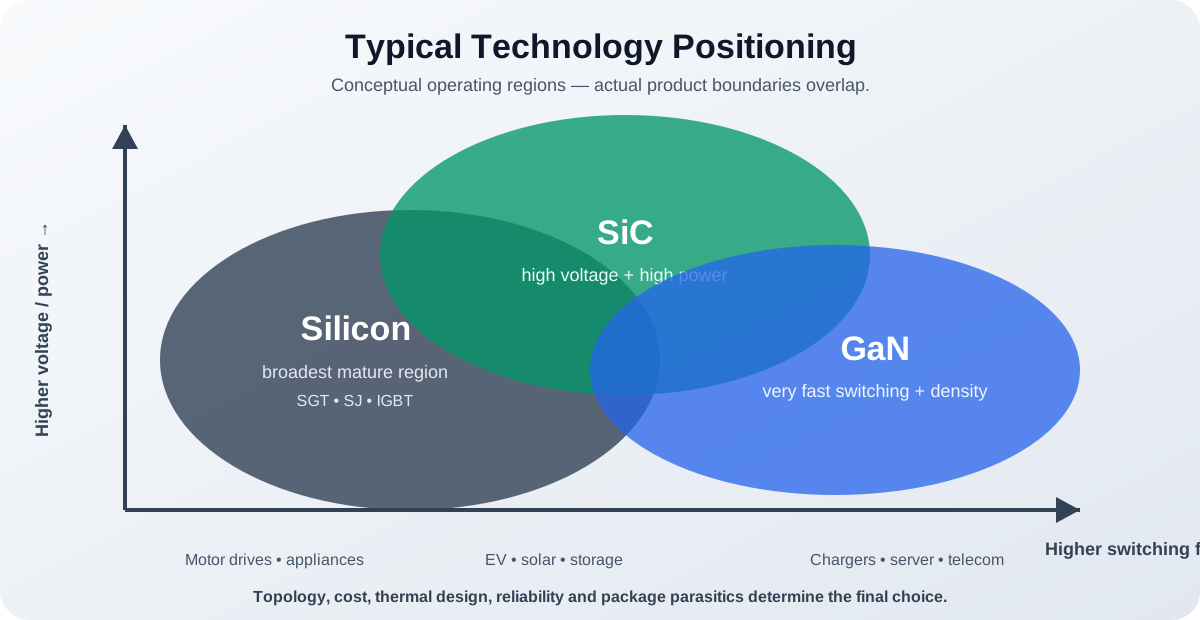
A simplified view is:
| Technology | Major strength | Typical application region |
|---|---|---|
| Silicon | Cost, maturity and broad applicability | Consumer, industrial, automotive, low-/medium-voltage and much high-voltage power |
| SiC | High voltage, high power and strong efficiency | EV, renewable energy, storage, industrial high-power conversion |
| GaN | Very fast switching and high power density | Chargers, adapters, server/telecom power and compact high-frequency conversion |
These are overlapping regions, not hard boundaries.
There are high-performance silicon solutions where SiC might technically work but not make commercial sense. There are SiC and GaN applications that overlap around similar voltage classes but optimize different system priorities.
Technology selection must therefore consider the whole operating window.
Why not use SiC or GaN everywhere?
If wide-bandgap devices are so capable, why does silicon remain dominant across large parts of the market?
Because every power design is also a cost, manufacturability and reliability decision.
Cost and ecosystem
Silicon benefits from decades of manufacturing scale and design experience.
If silicon already meets efficiency, thermal and size targets, the additional device cost or redesign effort of wide-bandgap technology may not create enough system value.
Gate-drive behaviour
SiC and GaN devices cannot always be treated like conventional silicon MOSFETs.
Important differences can include:
- recommended gate voltage;
- driver source/sink strength;
- negative gate-bias requirements in some SiC designs;
- very tight control of gate-loop inductance;
- protection strategy.
PCB layout
Fast switching creates very high dv/dt and di/dt.
Parasitic inductance and capacitance that were tolerable in a slower design can suddenly create:
- ringing;
- overshoot;
- false turn-on;
- EMI;
- reliability problems.
Wide-bandgap design therefore rewards compact current loops and disciplined PCB layout.
EMI is part of the trade-off
Faster edges reduce switching time but can make electromagnetic-interference control more demanding.
The designer may need to optimize:
- gate resistance;
- switching slew rate;
- common-mode current paths;
- shielding;
- filtering;
- PCB return paths.
The fastest possible edge is not always the best system solution.
Packaging becomes even more important
As semiconductor switching improves, package and interconnect parasitics become a larger part of overall behaviour.
A fast SiC or GaN device can be limited by:
- package inductance;
- PCB loop inductance;
- thermal interfaces;
- interconnect resistance.
This is driving increasing use of:
- Kelvin-source connections;
- low-inductance surface-mount packages;
- integrated driver/power stages;
- TOLL and related packages;
- top-side cooling;
- very compact gate-driver placement.
The boundary between device design, package design and PCB design is becoming increasingly blurred.
Silicon is still evolving
The rise of SiC and GaN does not mean silicon development has stopped.
SGT MOSFETs, Superjunction MOSFETs, advanced IGBTs and improved packages continue to move forward.
Instead of one technology replacing another completely, the power-semiconductor landscape is becoming more specialized.
A practical technology toolbox now includes:
SGT silicon MOSFETs → Superjunction MOSFETs → IGBTs → SiC → GaN
Each has operating regions where its combination of voltage, current, frequency, thermal behaviour, reliability and cost is compelling.
A practical technology-selection view
Consider silicon when:
- cost is highly important;
- voltage and frequency are well within mature silicon capability;
- supply maturity matters;
- existing design infrastructure already meets system targets.
Consider SiC when:
- voltage is high;
- power is substantial;
- switching and conduction loss have major system impact;
- thermal performance and cooling are important;
- higher system efficiency creates clear value.
Consider GaN when:
- switching frequency is a major design lever;
- very high power density is required;
- compact size is important;
- lower switching-related loss can enable smaller magnetics.
Key takeaway
The industry is not moving through a simple sequence of:
silicon → SiC → GaN.
It is moving toward a more specialized set of power semiconductor technologies.
Silicon continues to offer outstanding cost and performance across a huge portion of the market.
SiC extends power electronics strongly into demanding high-voltage and high-power systems.
GaN opens new possibilities where very fast switching and compact high-density conversion matter most.
The useful engineering question is therefore not:
“Which technology will win?”
It is:
“Which semiconductor technology allows this system to achieve the best balance of efficiency, size, thermal performance, reliability and cost?”